Buck Converter Design

Figure 1, Buck Converter
The buck converter comes standard with an LC output filter. The input current, on the other hand, is all chopped up by the main switch. This requires the DC bus powering the converter to have very low impedance over an unreasonably wide frequency spectrum to supply the super choppy input current without distortion. Because the input bus is more of a transmission line than an ideal voltage source, the choppy input current extends throughout this bus and injects noise to all the other components being powered by the bus. This is referred to as Conducted Emissions.
To combat these issues, an input filter is required. The input filter acts as a buffer between the bus as the converter, storing energy when the converter is drawing less power and releasing energy when the converter is drawing more power. From the DC-DC converter’s perspective, the input filter provides a low impedance interface to the power bus. With that in mind, it is important to make sure a filter is designed with its output impedance lower than the DC-DC converter’s input impedance over all frequencies.
For more info on input filter design, check out:

Figure 2, Buck Converter with Input Filter
Large Signal Model
Once you have your input filter, you can create your large signal model of your converter in two parts, on when the switch is on and one when it’s off. We will write state equations for both cases and average them into a single model, a technique known as state space averaging, developed by some guys you may remember, Dr. Middlebrook. (Link to middlebrook paper)
So what’s the big picture behind state space averaging? At first glance we are trying to develop a controller to control two different plants with the same output. But to develop a controller we need one plant and we need it to be linear, so how can we rig this? What we’re going to say is, if we make our controller response much slower than our switching frequency (which switches between our two plants), then we can just average our plats together and linearize them about an operating point. The operating point will be chosen by the desired nominal input and output voltages. The idea is that although the switching causes crazy non-linearity at high frequency, our much slower controller will be reacting to a slow (averaged) feedback from the output which is just what we’ve designed it for.
This main control loop is the slow voltage control loop. Later we’ll be adding a faster inner loop to control the current cycle by cycle. This is known as current mode control and it will improve our stability as well as reduce peak current stresses on components and create short circuit protection.
SW ON:

Figure 3, Switch On
Remember state equations are written in the form:
dx = Ax + Bu
y=Cx+Eu (note, most people write y=Cx+Eu but D is also duty cycle so we’ll use E)
The number of states is the number of energy storage components in the circuit (inductors and capacitors). Therefore the switch on circuit has 5 states. To select our states we’ll remember that:
IC = C*dVCdt
VL = L*dIL/dt
So our states will be currents of inductors and voltages of capacitors. Although you are free to define your state variables in which ever order you want, it is never a bad idea to define them from left to right according to the diagram.
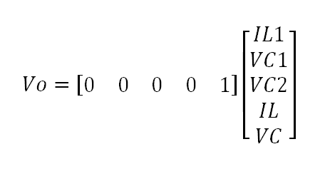
IL1, VC1, VC2, IL, VC
Because we have 5 states, we’ll need to generate 5 equations in terms of those 5 states plus the input. To do this we use KVL and KCL. Don’t make it hard on yourself, set up your diagram so the inductor currents are positive in the way they will actually flow and setup your capacitors so they are positive at the top and their currents flow into the positive/top (from + to -).
1) Vin - VC1 = L1* dIL1/dt => dIL1/dt = Vin/L1 - VC1/L1
2) IL1 = C1*dVC1/dt + (VC1 - VC2)/Rd + IL => dVC1/dt = IL1/C1 - VC1/(C1*Rd) + VC2/(C1*Rd) - IL/C1
3) (VC1 - VC2)/Rd = C2*dVC2/dt => dVC2/dt = VC1/(C2*Rd) - VC2/(C2*Rd)
4) VC1 – VC = L*dIL/dt => dIL/dt = VC1/L - VC/L
5) IL = C*dVC/dt + VC/Rl => dVC/dt = IL/C - VC/(RL*C)
For the states dx = Ax + Bu we have:
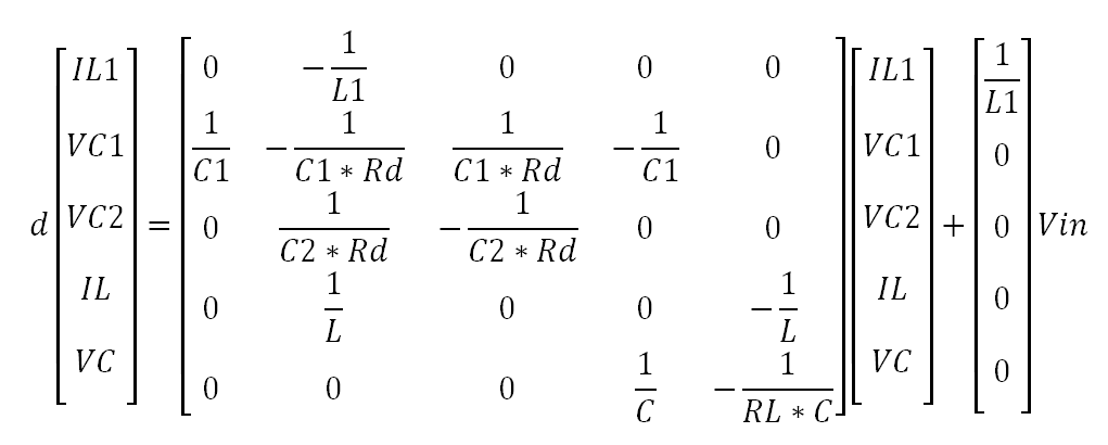
For the output y=Cx+Eu (note that Eu = 0) we have:
SW OFF:

Figure 4, Switch Off
For this one we will set up the polarities according to the actual system. When the switch is off, the polarity of the inductor flips and both the inductor and the capacitor now supply current out of their positive lead (- to +). Our states will be from left to right:
IL, VC
We have two states or unknowns, so we need two equations. Using KCL and KVL:
IL - C*dVC/dt = VC/Rl => dVC/dt = IL/C - VC/(Rl*C)
Vo = VC = -L*dIL/dt => dIL/dt = -VC/L
For the states dx = Ax + Bu we have:
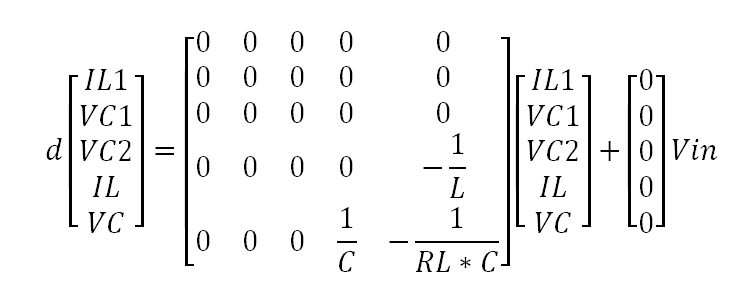
For the output y=Cx+Eu (note that Eu = 0) we have:
Averaged Large Signal Model
Now that we have our large signal models we will average them proportional to our duty cycle. We will use A1, B1, C2 and D1 for when the switch is on and A2, B2, C2 and D2 matrices for when the switch is off.
d = steady state duty cycle (constant for a fixed input, fixed output converter)
dx = derivative of x matrix
dx = Ax + Bu
y=Cx+Eu
A => A1*d + A2*(1-d)
B => B1*d + B2*(1-d)
C => C1*d + C2*(1-d)
E => E1*d + E2*(1-d) = [0]
We can just leave these equations in this form for now, no need to multiply out the full matrices again.
Small Signal Model
For the small signal model we’ll split each term in x into two parts, a large signal or steady state part and a small signal or controllable part.
d => D + d̂
x => X+x̂
u => U+û
d(X + x̂) = [A1*(D + d̂) + A2*(1 - D - d̂)]*(X + x̂) + [B1*(D + d̂) + B2*(1 - D - d̂)]*(U + û)
Y + ŷ = [C1*(D + d̂) + C2*(1 - D - d̂)]*(X + x̂) + [E1*(D + d̂) + E2*(1 - D - d̂)]*(U + û)
So now we have to think about what this equation represents and we’ll be able to simplify it. What we want to describe is how small changes in the duty cycle around the steady state operating point change the output voltage. With that in mind we first notice that d(X) is the derivative of the steady state X, which by definition is zero.
dX = 0 = A*X + B*U
d(X + x̂) = d(X) + d(x̂) = d(x̂)
The next thing to notice is that we’re going to have terms that describe small signal effects on other small signals, which we really don’t care about. What we want to base our control on is the small signal effects on the averaged model. Therefore any terms like x̂*d̂ can be neglected.
So for the states we have:
d(X + x̂) = A1*D*X + A1*D*x̂ + A1*d̂*X + A1*d̂*x̂ + A2*(1 - D)*X + A2*(1 - D)*x̂ - A2*d̂*X - A2*d̂*x̂
+ B1*D*U + B1*D*û + B1*d̂*U + B1*d̂*û + B2*(1 - D)*U + B2*(1 - D)*û - B2*d̂*U - B2*d̂*û
Remember:
dX = 0
A1*D*X + A2*(1 - D)*X + B1*D*U + B2*(1 - D)*U = A*X + B*U = 0
A1*D*x̂ + A2*(1 - D)*x̂ + B1*D*û + B2*(1 - D)*û = A*x̂ + B*û
So we can simplify to:
d(x̂) = A*x̂ + B*û + [(A1 - A2)*X + (B1 - B2)*U]*d̂
For the output we have the exact same procedure leading to:
ŷ = C*x̂ + E*û + [(C1 - C2)*X + (E1 - E2)*U]*d̂
But for us E = 0 so:
ŷ = C*x̂ + (C1 - C2)*X*d̂
We can see form these equations that only the right part depends on d̂, so that is the part that the controller is actually able to effect.
Plant Design:
At this point we’re going to need to select the component values for the main power stage or plant of the converter. To do this we’re going to use the steady state part of the model:
d => D
d(x) = Ax + Bu => 0 = A*X + B*U => X = -A^-1*B*U
y = Cx + Eu => Y = C*X => Y = -C*A^-1*B*U
First we choose our input voltage and our output voltage:
Vin = 20V
Vout = 5V
Vout-ripple <= 5%
F = 100KHz
There’s a good article on how to select components:
http://powerelectronics.com/dc-dc-converters/buck-converter-design-demystified
Inductor:
If we assume we’re in continuous conduction mode (CCM) and we have ideal diodes and switches (with no voltage drop or on resistance) we can calculate L with:
L = (Vin-max - Vo)*Vo/(Vin-max*F*Ir)
Ir = ripple current (inductor) = 0.2*Io-max to 0.5*Io-max
Higher values of Ir give a quicker transient response and a smaller inductor, while lower values give better filtering.
ILpeak = Io-max + Ir/2
Choose a saturation current rating with a 20% margin over ILpeak.
Capacitor:
For the output capacitor, we’re going to let the max overshoot determine the capacitance and the max ripple determine the ESR. Because our control model assumes 0 ESR we should be OK but it’s important to note that lower ESR’s make it easier for the system to be unstable. This is more relevant when dealing with a packaged controller. For the max overshoot, we’ll look at the worst case where the inductor is fully charged up just before the load is completely removed. In this scenario we’ll have all the stored energy from the inductor get transferred to the capacitor and we’ll set a limit Vo-peak that is the max output voltage during an overshoot condition. A reasonable choice for Vo-peak might be 5% or 1.05*Vo.
Ec = 0.5 * C * (Vo-peak^2 – Vo^2)
El = 0.5 * L * ILpeak^2
Ec = El => C * (Vo-peak^2 – Vo^2) = L * ILpeak^2
C = L*ILpeak^2/(Vo-peak^2 – Vout^2)
Since most caps are +/- 20%, add at least a 20% margin to the selected capacitor value.
Vo-ripple = Vc-ripple + Vc-esr-ripple
Vc-ripple = (charge/cycle) / C
charge/cycle = Ir/(2*F) (assuming a triangle wave ripple)
Vc-esr-ripple = Ir * ESR
Vo-ripple = Ir/(2*C*F) + Ir*ESR
ESR = Vo-ripple/Ir – 1/(2*C*F)
A good choice for Vo-ripple is 2% or 0.02*Vo
Diode:
Pd = (1-D)*Io*Vd = (1 - Vo/Vin)*Io*Vd
Pd = power rating of diode
Vd = forward voltage drop of diode
Main Switch:
Tj-max < 120C (junction temp)
Ta-max < 60C (ambient temp)
Tj-rise = Tj-max – Ta-max < 60C
Pq = Tj-rise / TRj
TRj = junction thermal resistance (from datasheet, use 60C/watt for std SO-8 pack on 1 sq-in 1 oz copper pwb)
Pq = Pq-sw + Pq-on
Pq-on = (Vo/Vin)*Io^2*Rds-on-hot
Rds-on-hot can be found from the datasheet. If it only lists ambient it can be estimated with:
Rds-on-hot = (1 + 0.005*(Tj-max – 25C))*Rds-on-ambient
Pq-sw is hard to determine. You can just say Pq = 2*Pq-on if you can’t find it on some graphs in the datasheet. Just remember this is a really loose estimate since it’s actually linearly proportional to frequency.
Input Filter:
We want the cutoff frequency of the control loop to be roughly 1 order of magnitude below the main switching frequency. Likewise we want the cutoff frequency of our input filter roughly an order of magnitude below our control loop cutoff. Therefore if we had a 100KHz switching frequency we might have a 10KHz voltage control loop and a 1KHz input filter.
For C1 a good rule of thumb is 10uF per amp of ripple. For the input the ripple would be Iin during the switch on cycle, which is equivalent to Io (because when the switch is on, Iin = Io). So what we’re saying is that we want a filter with a fixed cutoff frequency for 100 X less than the switching frequency, but we need to adjust our inductor and capacitor sizes for different currents. For a higher current converter, we want a larger capacitor and a smaller inductor. For a lower current converter we want a smaller capacitor and a larger inductor. The reason is that a larger inductance is created by more turns of a smaller wire which leads to a smaller current rating, while a larger capacitor is made by incorporating larger plate surface that leads to a larger current rating.
C1 = 10uF * Io
Another way to show it:
C1 = 10uF * Iin / D
D = Vo / Vin
Vin*Iin = Vo*Io = Vo^2/RL =>
Iin = Vo^2/(Vin*RL)
C1 = (10uF * Vo^2/(Vin*RL)) / (Vo / Vin) = 10uF * Vo^2*Vin/(Vin*RL*Vo) = 10uF * Vo / RL = 10uF * Io
Fco = 1/(2*pi sqrt(L1*C1)) = F/100 => 100/F = 2*pi sqrt(L1*C1) => (100 / (F*2*pi))^2 = L1*C1
L1 = (50 / (F*pi))^2 /C1
n = C2 / C1 = (Rof^2/Zo)*sqrt(1 + 4*Zo^2/Ro^2)
Zo = peak output impedance
Rof = sqrt(L1/C1) = (characteristic impedance of low pass filter without damped element)
So you can pick a value for Zo and solve for n, however, the point of C2 is that you’re putting a resistor in parallel with C1 and using C2 as a DC-block. So as long as C2 is a few times larger than C1 you should be good. Something on the order of C2 = 5*C1 (n = 5) should be fine.
Rd = Rof*sqrt((2+n)*(4+3*n)/(2*n^2*(4+n)))
Controller design:
For the controller design we’re going to start with the outer voltage loop. We’re going to do a PID controller and use the root-locus to verify stability. Another method is to use bode plots to determine gain and phase margins, but this only works for “non-minimum phase systems” and does not necessarily work for systems with poles in the right half plane, which the buck may have. The PID has 3 gain values so unfortunately it can’t be easily designed using the root locus (root locus is plotted for a single gain value). The nice thing about PID, however, is that you can easily tune it by trial and error. There are other more sophisticated control algorithms that we may talk about in future articles, but the simplest is PID, and there are several methods that standardize the tuning procedure that you can google for. The goal is not to find the optimal response, but to find a stable, acceptable response based on some design spec.

Figure 5, Generic Closed Loop Controller
Closed Loop TF = K*Gc*Gp / (1 + K*Gc*Gp*H)
Characteristic Equation (CE): 1 + K*Gc*Gp*H = 0
Roots of CE = closed loop poles
@ zeroes, K = infinity
@ poles, K = 0
PID Laplace:
Proportional (P) => Kp
Integral (I) => Ki / s
Dirivative (D) => Kd*s
PID = Kp + Ki / s + Kd*s

Figure 6, PID Frequency Response
The PID has 3 parts. The Integral is the low frequency component and it guarantees the system will eventually converge to a zero error state. The proportional is the mid-frequency and helps the system respond faster. The derivative part reacts fast to high frequency changes. This part as you can see brings the gain back up at high frequencies, decreasing the gain margin. Therefore if you can meet your requirements with just the I and P parts, you are free to leave off the D.
Matlab/Scilab/Octage Procedure:
1) Define model, control and feedback functions Gp, Gc and H.
2) Iteratively tune the PID
a. Choose values for Kp, Ki and Kd
b. Run step response
c. If step looks good, you’re done, if not go back to a.
3) Plot root loci
a. Preferably all poles and zeros are in the left half plane.
b. At least for a gain of 1 you must be in the left half plane.

Figure 7, PIDClosed Loop Controller
Now we can use Scilab to plot the step response:
VOpeak = 1.05*Vo;
C = L*ILpeak^2/(VOpeak^2 – Vo^2);
Iin = Vo^2/(Vi*RL);
C1 = 10e-6*Io;
L1=(50/(F*%pi))^2/C1;
n=5;
C2=n*C1;
Rof = sqrt(L1/C1); //characteristic impedance of LC filter
Rd = Rof*sqrt((2+n)*(4+3*n)/(2*n^2*(4+n))); //Damper

//STEADY STATE MODEL OF THE BOOST CONVERTER
//given by As, Bs, Cs and Ds matrices

As1 = [0 -1/L1 0 0 0;
1/C1 -1/(C1*Rd) 1/(C1*Rd) -1/C1 0;
0 1/(C2*Rd) -1/(C2*Rd) 0 0;
0 1/L 0 0 -1/L;
0 0 0 1/C -1/(RL*C)];
Bs1 = [1/L; 0; 0; 0; 0];

Cs1 = [0 0 0 0 1];
Es1 = [0];

As2 = [0 0 0 0 0;
0 0 0 0 0;
0 0 0 0 0;
0 0 0 0 -1/L;
0 0 0 1/C -1/(RL*C)];
Bs2 = [0; 0; 0; 0; 0];

Cs2 = [0 0 0 0 1];
Es2 = [0];

As = As1*D + As2*(1 - D);
Bs = Bs1*D + Bs2*(1 - D);
Cs = Cs1*D + Cs2*(1 - D);
Es = Es1*D + Es2*(1 - D);

//Smal Signal Model
IL1 = Vo*Vo/(Vi*RL); //steady state input current
VC1 = Vi;
VC2 = Vi;
IL = Vo/RL;
VC = Vo;

Xs = [IL1; VC1; VC2; IL; VC]; //steady state X
Us = Vi;
ViHatTerm = Bs*Us; //The B matrix for input = Vin
dHatTerm = ((As1-As2)*Xs+(Bs1-Bs2)*Us); //The B matrix for input = d

//A => As, B => dterm, C => Cs, E => eterm
eterm = (Cs1-Cs2)*Xs;

sys = syslin('c', As, ViHatTerm, Cs, eterm); //'c' = continuous time

s=poly(0,'s'); //define s to be used for lapalce notation

Kd = 0.00001; //0.00001
Ki = 5; //5
Kp = 0.005; //0.005

//Model of the CONTROL SYSTEM
ctrl = syslin('c', Kd*s*s+Kp*s+Ki, s); //continuous, numerator=1, denomerator=s

//Feedback H
H = syslin('c', 1, 1); //continuous, numerator=1, denomerator=1

ol=sys*ctrl;  //open loop transfer function

cl = ol /. H; //slash-dot does the closed loop with fb H

//Step Response
t=0:1e-5:0.1; //setup graph start time, step size, stop time

cs=csim('step',t,cl); //calc step response
//if this fails to converge, decrease the step size via. t

clf; //clear and reset current graph
plot2d('nn', cs)
xlabel("Time (uS)");
ylabel("Vo/Vo-ref");
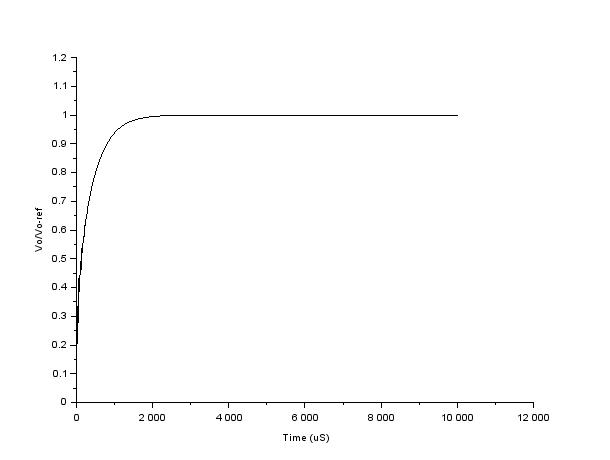
Figure 8, Closed Loop Step Response
clf; //clear and reset current graph
evans(cl, 100) //display root locus of the closed loop tf
sgrid();
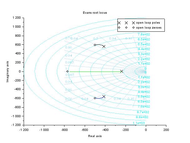
Figure 9, Root Locus